Artem Voloskovets
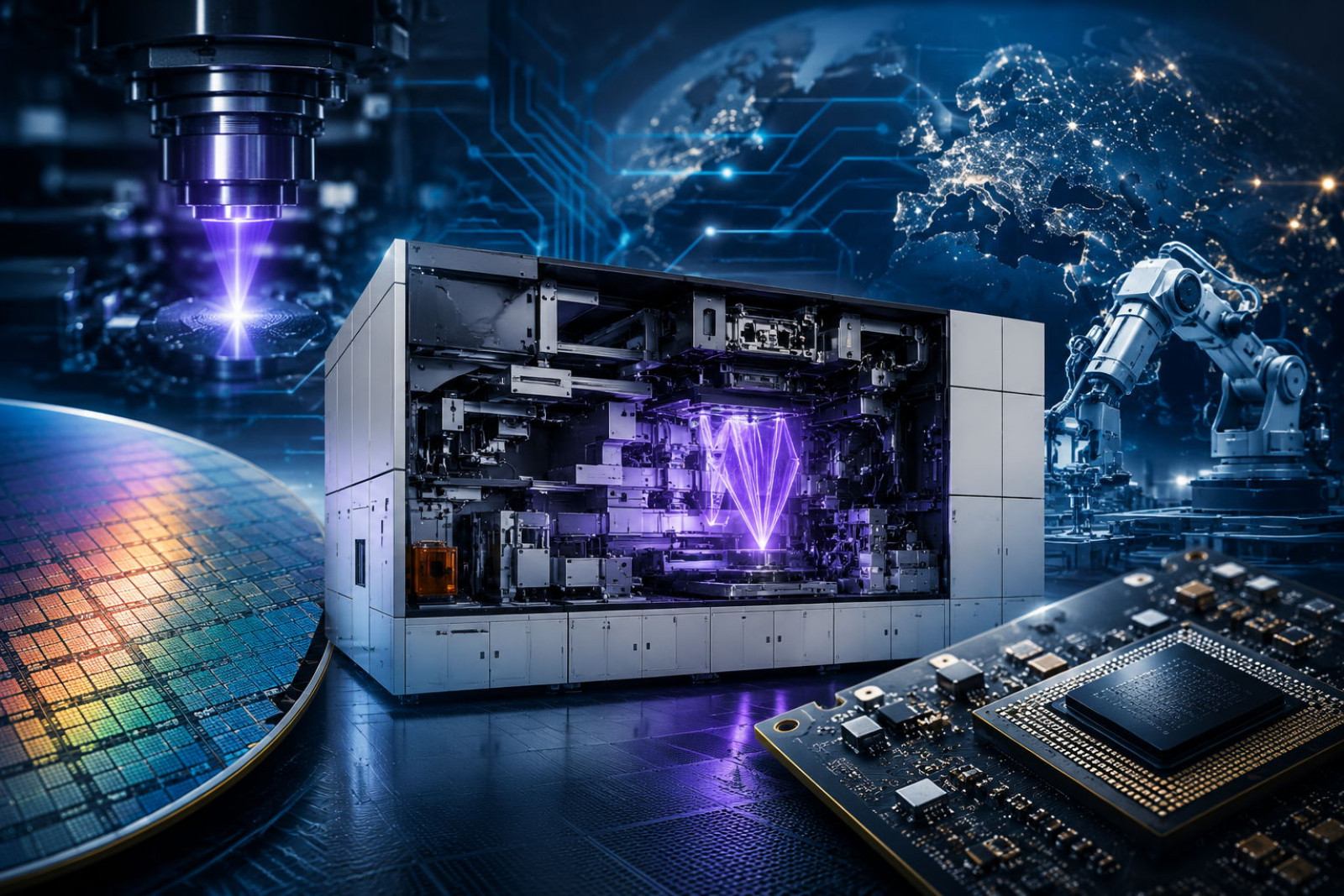
- By the Numbers
- A Market With No Alternative
- Why Consumers Have Never Heard of ASML
- Every AI Model Starts Here
- Editor's Note
- More Than a Machine
- Fact Box: Why €350 Million Makes Sense
- Timeline: The Early Years
- Entering a Market Nobody Wanted to Leave
- Market Share in the 1980s
- Why Nikon Looked Unbeatable
- The Limits of Incremental Progress
- Sidebar: Moore's Law Was Never a Law
- The Bet Nobody Wanted to Make
- The Cost of Delaying a New Technology
- Why EUV Looked Impossible
- Betting Against the Market
- The Partnership Model That Changed Everything
- Customers Became Investors
- Fifteen Years Before the First Real Success
- Inside the World's Most Complex Machine
- From Digital Design to Physical Reality
- One Exposure, Thousands of Engineering Problems
- Why Ordinary Glass Becomes Useless
- Precision Beyond Human Intuition
- The Cleanest Manufacturing Environment on Earth
- Why Vacuum Matters
- Software: The Invisible Machine Inside the Machine
- More Than the Sum of Its Parts
The €350 Million Machine
In early 2024, a convoy carrying one of the world's most valuable industrial machines left the Dutch town of Veldhoven for a semiconductor fabrication plant overseas. The cargo required dozens of specially designed containers, coordinated logistics across several countries, and months of installation after arrival. Unlike an aircraft or a power plant turbine, the machine could not simply be switched on once delivered. Hundreds of engineers would spend months assembling, calibrating and testing it before it produced a single usable silicon wafer.
The price of that machine exceeded €350 million.
At first glance, the figure seems irrational. Even the most sophisticated CNC systems, aircraft engines or MRI scanners cost only a fraction of that amount. Yet ASML's latest High-NA EUV lithography system has become so valuable that leading chipmakers are willing to order it years before delivery, despite knowing that production schedules may change and installation will temporarily disrupt their factories.
The obvious question is not why the machine is expensive.
The real question is why companies such as Intel, TSMC and Samsung cannot afford not to buy it.
By the Numbers
| Metric | High-NA EUV System |
| Approximate price | €350M+ |
| Weight | ~150 tonnes |
| Height | Comparable to a two-story house |
| Shipping containers | More than 250 |
| Individual components | 100,000+ |
| Assembly time | 4–6 months |
| Tin droplets fired every second | 50,000 |
| Customers | Intel, TSMC, Samsung |
A Market With No Alternative
Technology markets are rarely dominated by a single supplier. Even companies with commanding positions, Microsoft in enterprise software, Nvidia in AI accelerators or TSMC in contract chip manufacturing, operate in competitive environments. Customers may prefer one vendor over another, but alternatives exist.
Lithography is different.
Today, ASML is the only company capable of supplying extreme ultraviolet (EUV) lithography systems for high-volume semiconductor manufacturing. Neither Nikon nor Canon, once dominant names in optical lithography, has a commercial EUV platform. Chinese manufacturers remain years behind in this field, while no American company competes directly in advanced lithography equipment.
This makes ASML's position unusual even by technology industry standards. The company is not simply a market leader; it occupies a technological niche that no competitor has successfully entered. For manufacturers building chips at the most advanced process nodes, choosing ASML is not a strategic decision—it is the only practical option.
The Hidden Position of ASML
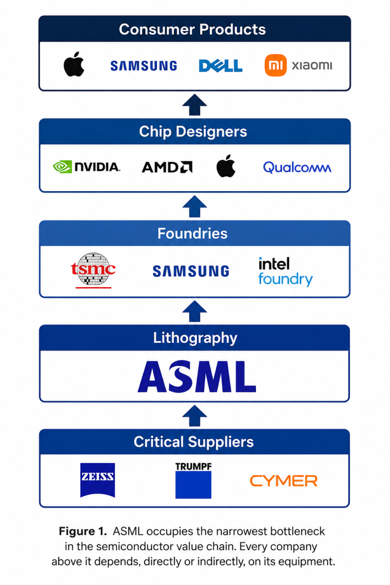
Figure 1. ASML occupies the narrowest bottleneck in the semiconductor value chain. Every company above it depends, directly or indirectly, on its equipment.
Why Consumers Have Never Heard of ASML
The world's largest technology companies spend billions of dollars building consumer brands. Apple promotes new iPhones through global marketing campaigns. Nvidia dominates discussions about artificial intelligence. TSMC regularly appears in financial headlines as investors track demand for advanced chips.
ASML does none of these things because its customers are not consumers. The company sells fewer than a hundred advanced lithography systems each year, and each one is built for a semiconductor manufacturer rather than a retailer. There are no product launches streamed online, no advertising campaigns and no retail distribution network. Most people interact with ASML's technology every day without realizing it.
This invisibility has created an unusual paradox. Although ASML is among Europe's most valuable technology companies, its name recognition outside the semiconductor industry remains remarkably low. Yet nearly every modern processor powering smartphones, data centres, autonomous vehicles or AI clusters has passed through a production line built around ASML equipment.
Every AI Model Starts Here
The recent boom in artificial intelligence has focused public attention on software. Large language models, AI assistants and generative image tools dominate headlines, while companies developing them compete to announce larger models and higher benchmark scores.
Far less attention is paid to the infrastructure that makes those models possible.
Before an AI system answers a question, billions of transistors must first be manufactured. Those transistors become GPUs, CPUs, high-bandwidth memory chips and networking processors. Together they form the computing clusters that train and run modern AI models.
Each stage depends on the one before it.
| Layer | Example Companies |
| AI Applications | OpenAI, Anthropic, Microsoft |
| AI Hardware | NVIDIA, AMD |
| Chip Manufacturing | TSMC, Samsung, Intel |
| Lithography | ASML |
The further down this chain one looks, the fewer companies remain. At the application layer there are hundreds of competitors. At the hardware layer there are several global leaders. Advanced manufacturing is concentrated in only a handful of foundries.
At the lithography layer, the list effectively ends with one company.
Editor's Note
Investors often describe Nvidia as the company powering the AI revolution. That statement is accurate — but incomplete. Nvidia designs the processors. TSMC manufactures them. ASML provides the only machines capable of producing many of the critical transistor layers inside those processors.
More Than a Machine
Calling an EUV lithography system a "machine" understates its complexity. It is better understood as an integrated manufacturing platform that combines optics, plasma physics, precision mechanics, computational control systems and advanced materials engineering.
Unlike conventional production equipment, an EUV system is assembled from components supplied by hundreds of specialised companies. The mirrors come from Germany's Carl Zeiss SMT. The high-power laser system relies on technology developed by Cymer, now an ASML subsidiary. Precision positioning systems, vacuum chambers, sensors and control electronics are sourced from an international network of suppliers, many of which have spent decades refining components that cannot easily be replaced.
This distributed ecosystem is one of ASML's greatest competitive advantages. While rivals could theoretically invest billions of euros to develop their own lithography systems, replicating the supplier network that supports ASML would require rebuilding decades of accumulated expertise across multiple industries.
Fact Box: Why €350 Million Makes Sense
The price reflects far more than manufacturing costs.
- More than 40 years of research and development.
- Hundreds of specialised suppliers.
- Components manufactured to tolerances measured in fractions of a nanometre.
- Years of software development for process control.
- Continuous servicing and upgrades throughout the machine's operating life.
- Extremely low production volumes compared with almost any other industrial equipment.
The economics are straightforward. A single leading-edge semiconductor fabrication plant may cost $20–30 billion to build. In that context, paying several hundred million euros for the equipment that enables the entire facility to produce next-generation chips becomes a rational investment rather than an extraordinary expense.
How a Small Dutch Startup Defeated Japan's Giants
In 1984, few people inside the semiconductor industry would have predicted that the future of chip manufacturing would be shaped by a newly created joint venture operating from a collection of temporary buildings in the Netherlands.
At the time, the balance of power looked almost unchangeable.
Japan dominated semiconductor manufacturing. Japanese companies produced nearly half of the world's chips, while firms such as Nikon and Canon had established themselves as the undisputed leaders in lithography equipment. Their systems powered production lines across Asia, Europe and the United States, and decades of optical engineering experience made them appear almost impossible to challenge.
Against that backdrop, ASML entered the market with no established customer base, limited financial resources and virtually no international reputation.
The company was born as a joint venture between Philips, one of Europe's largest electronics manufacturers, and ASM International, a Dutch supplier of semiconductor production equipment founded by entrepreneur Arthur del Prado. Philips needed an external supplier capable of developing lithography systems, while ASM saw an opportunity to expand beyond its existing product portfolio. Neither partner expected the venture to redefine an entire industry.
The first ASML office reflected those modest ambitions. Engineers worked from temporary modular buildings erected beside a Philips facility in Eindhoven. Early development teams operated with a fraction of the budget available to Japanese competitors, and their first products struggled to convince customers already comfortable buying equipment from Nikon or Canon.
Timeline: The Early Years
| Year | Milestone |
| 1984 | ASML founded as a Philips–ASM joint venture |
| 1985 | First prototype lithography system completed |
| 1988 | First international customers |
| 1995 | Listed on NASDAQ and Amsterdam Stock Exchange |
| 2001 | Acquisition of Silicon Valley Group (SVG) |
| 2000s | Begins large-scale investment in EUV |
Entering a Market Nobody Wanted to Leave
The lithography business has never resembled the consumer electronics industry, where a successful product can quickly attract new competitors. Chip manufacturers invest billions of dollars in fabrication plants, and every new piece of production equipment must demonstrate exceptional reliability before it is trusted with commercial manufacturing.
For a company attempting to enter this market, technological excellence alone is not enough. Customers must believe that a supplier will still exist ten or twenty years later, continue servicing equipment, provide software updates and develop the next generation of tools. In other words, semiconductor manufacturers do not simply buy machines—they buy decades of technological continuity.
This created a formidable barrier for ASML. Convincing a customer to replace an established supplier meant asking them to risk production yields worth billions of dollars. Even a marginal decrease in manufacturing performance could erase years of expected savings.
Instead of competing on price, ASML focused on engineering flexibility. The company introduced modular system architectures that simplified maintenance and upgrades, allowing customers to improve existing equipment rather than replacing it entirely. This approach gradually reduced the total cost of ownership and gave manufacturers a practical reason to evaluate a newcomer.
The strategy did not produce immediate success, but it established a pattern that would define ASML for decades: invest aggressively in technologies that competitors considered too risky or too expensive.
| Company | Position |
| Nikon | Market leader |
| Canon | Strong global competitor |
| GCA (US) | Declining |
| Ultratech | Specialty applications |
| ASML | Emerging challenger |
Observation: At this stage, there was little indication that ASML would eventually dominate the industry. Nikon appeared to be the long-term winner, supported by Japan's powerful semiconductor ecosystem and decades of expertise in precision optics.
Why Nikon Looked Unbeatable
Looking back with the benefit of hindsight, ASML's rise can seem inevitable. It was anything but.
By the late 1980s Nikon possessed nearly every competitive advantage analysts typically associate with market leadership. The company had deep expertise in optical engineering, a strong balance sheet, long-standing customer relationships and an established reputation for manufacturing precision. Canon, meanwhile, had built its own formidable position, leveraging technologies developed for cameras and imaging systems.
Both companies improved lithography systems incrementally, focusing on higher throughput, better image quality and greater production reliability. Given the industry's trajectory at the time, this strategy made perfect sense. Semiconductor manufacturers were still shrinking transistor dimensions, but the pace appeared manageable within the existing technological framework.
Few engineers believed that optical lithography itself would eventually reach a physical limit.
That assumption would prove to be the industry's greatest miscalculation.
Most technological leaders fail not because they stop innovating, but because they continue improving technologies that are approaching their natural limits.
This observation appears repeatedly in studies of industrial disruption, from mechanical calculators to photographic film. Lithography would eventually follow the same pattern.
The Limits of Incremental Progress
Semiconductor manufacturers relied on a simple principle: if smaller transistors required higher resolution, engineers could continue improving optical systems. Better lenses, shorter wavelengths and increasingly sophisticated process control delivered predictable gains year after year.
This approach became known inside the industry as the "extend rather than replace" philosophy.
It worked remarkably well.
Deep ultraviolet lithography evolved through multiple generations, and engineers repeatedly postponed the need for a fundamentally different technology. Techniques such as immersion lithography and multiple patterning squeezed additional performance from existing equipment, allowing manufacturers to continue following Moore's Law without abandoning familiar production methods.
However, every improvement came at a cost.
Multiple patterning required additional exposure steps, increasing manufacturing time and reducing throughput. More complex process flows demanded tighter alignment tolerances and introduced new opportunities for defects. What initially appeared to be elegant engineering gradually became an increasingly expensive workaround.
By the early 2000s, the industry faced an uncomfortable reality: each additional transistor generation required disproportionately greater effort.
The economics that had sustained semiconductor scaling for decades were beginning to break down.
Sidebar: Moore's Law Was Never a Law
Moore's Law is often described as the observation that the number of transistors on a chip doubles approximately every two years.
In practice, it functioned less as a law of physics than as an industry roadmap.
Equipment manufacturers, chip designers, material suppliers and software developers coordinated their investments around the expectation that transistor density would continue increasing. When lithography began approaching its physical limits, the challenge extended far beyond optics—it threatened the planning assumptions underpinning the entire semiconductor industry.
The Bet Nobody Wanted to Make
Around the same time, researchers were exploring an alternative that many executives considered unrealistic.
Instead of extracting incremental improvements from deep ultraviolet lithography, they proposed building an entirely new manufacturing platform based on extreme ultraviolet light.
The concept promised dramatically higher resolution. It also required solving problems that many experts regarded as practically impossible. Ordinary lenses would no longer work. Air itself would absorb the light. Even dust particles could disrupt the optical path.
No suitable light source existed. Perhaps most importantly, no company could estimate with confidence whether the technology would ever become commercially viable. For established market leaders, the incentives were clear. Continue refining profitable products and wait until EUV matured.
ASML made the opposite decision. Rather than protecting its existing business, it committed billions of euros to a technology that might never work. At the time, the decision appeared reckless. In retrospect, it became the defining strategic investment in the history of the semiconductor equipment industry.
The €10 Billion Bet That Had No Guarantee of Success
By the late 1990s, the semiconductor industry faced a dilemma that was becoming increasingly difficult to ignore. For decades, engineers had relied on the same formula: make optical systems better, shorten the wavelength of light, improve process control and continue shrinking transistors. Every generation of lithography equipment had extended Moore's Law a little further, reinforcing the belief that innovation would continue through incremental improvements rather than radical breakthroughs.
The problem was that physics was beginning to impose limits that engineering alone could no longer overcome.
Lithography had always depended on one fundamental relationship: the smaller the wavelength of light, the smaller the features that could be projected onto a silicon wafer. Throughout the 1980s and 1990s, manufacturers steadily reduced wavelengths from mercury lamps to excimer lasers operating at 248 nanometers and later 193 nanometers. Each transition required enormous investments but delivered another decade of progress.
By the end of the 1990s, however, there was no obvious successor.
The industry had squeezed almost everything it could from deep ultraviolet lithography. Engineers introduced immersion systems, placing a thin layer of ultra-pure water between the lens and the wafer to improve resolution. When that was no longer enough, they developed multiple-patterning techniques that exposed the same wafer several times instead of once. The technology continued to advance, but every improvement came at the cost of additional complexity, lower throughput and rapidly rising manufacturing expenses.
A growing number of researchers concluded that the industry's roadmap was becoming economically unsustainable. Moore's Law was not failing because transistor design had stopped improving; it was becoming prohibitively expensive to print the next generation of transistors.
The Cost of Delaying a New Technology
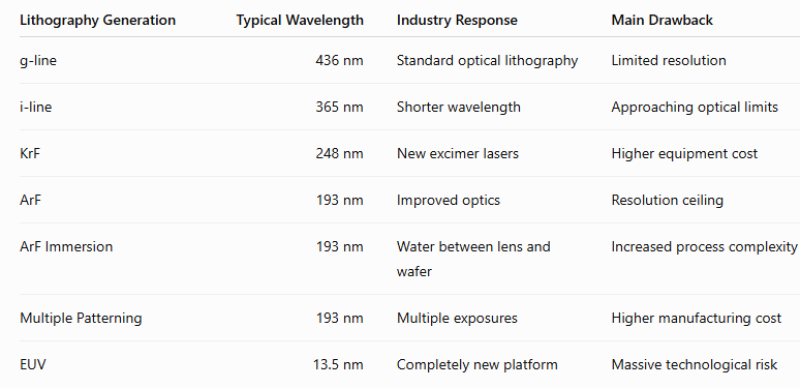
The table illustrates an important pattern. Until EUV, every new generation represented an evolution of existing technology. EUV was different. It was not another upgrade—it required rewriting almost every assumption on which modern lithography had been built.
Why EUV Looked Impossible
If someone proposed building an aircraft without aluminum, or a submarine that could not enter water, most engineers would dismiss the idea immediately. Extreme ultraviolet lithography sounded almost equally unrealistic.
The first problem was the light itself.
Unlike visible or deep ultraviolet light, radiation at 13.5 nanometers is absorbed by almost everything it encounters. Air absorbs it. Glass absorbs it. Most materials absorb it. Conventional optical systems therefore become useless. The very components that had defined lithography for decades, precision lenses, could not be used at all.
That forced researchers into unfamiliar territory. Instead of transmitting light through glass, they would need to reflect it using mirrors so precise that even atomic-scale imperfections could distort the final image.
The second challenge was generating the light source. Semiconductor factories required a stable beam powerful enough to expose thousands of wafers every day. Yet no commercially viable source of extreme ultraviolet radiation existed.
The third challenge involved contamination. At wavelengths measured in nanometers, microscopic particles invisible to the human eye become catastrophic defects. Even molecular contamination gradually reduces mirror reflectivity, lowering system performance over time.
None of these problems had straightforward solutions. Collectively, they represented one of the most ambitious engineering programs ever attempted by a commercial company.
Engineering Reality Check
To manufacture advanced chips using EUV, engineers had to solve all of the following problems simultaneously:
- Generate stable 13.5 nm radiation.
- Operate inside an ultra-high vacuum.
- Replace refractive optics with multilayer mirrors.
- Maintain nanometer-scale positioning accuracy during wafer exposure.
- Eliminate contamination that gradually damages optical surfaces.
- Deliver sufficient throughput for commercial semiconductor production.
Solving only one of these problems would not create a viable product. Every subsystem had to work reliably at the same time.
Betting Against the Market
During the early years of EUV research, skepticism extended well beyond academic circles. Investors questioned whether the technology would ever become commercially viable. Customers worried that decades of research might ultimately produce nothing usable. Even within the semiconductor industry, many executives believed that conventional lithography could continue evolving through increasingly sophisticated process techniques.
From a business perspective, delaying investment appeared rational. Existing lithography systems generated reliable profits. Customers continued placing orders. No immediate competitive threat existed. For established market leaders, protecting the current business looked safer than financing a technology whose commercial future remained uncertain.
ASML reached a different conclusion.
Rather than treating EUV as a research project, management increasingly viewed it as the company's future. If conventional lithography eventually reached its physical limits, whoever mastered EUV first would define the next era of semiconductor manufacturing.
The decision fundamentally changed the company's strategy. Research budgets expanded. Long-term partnerships became essential. Development timelines stretched from years into decades.
ASML was no longer trying to build a better lithography machine.
It was attempting to reinvent lithography itself.
The Partnership Model That Changed Everything
One of ASML's most important strategic decisions had little to do with optics. Instead of trying to develop every critical technology internally, the company assembled an ecosystem of specialist partners whose expertise often exceeded its own.
That approach contrasted sharply with the vertically integrated philosophy common in industrial manufacturing. Rather than becoming the world's best optics company, ASML partnered with the world's best optics company. Rather than building every laser internally, it acquired and integrated the industry's leading laser expertise.
The result was a supply chain unlike almost any other in advanced manufacturing.
| Partner | Core Expertise | Why It Matters |
| Carl Zeiss SMT | Precision mirrors | EUV optics depend entirely on mirror quality |
| Cymer | High-power laser systems | Generates the plasma light source |
| TRUMP | FIndustrial laser technology | Supports laser amplification and stability |
| Hundreds of precision suppliers | Motion systems, sensors, mechatronics | Enable nanometer-scale positioning |
This distributed innovation model became one of ASML's greatest competitive advantages. Each partner invested for years, often decades, in technologies that had little commercial value outside EUV lithography. As those capabilities matured together, the network itself evolved into a competitive moat.
Today, replicating ASML means more than copying a machine. It would require rebuilding an industrial ecosystem spanning several countries and thousands of highly specialized engineers.
People often ask whether another company can build an EUV machine. The better question is whether another ecosystem can. Semiconductor industry analyst
Customers Became Investors
Perhaps the clearest indication that EUV had become strategically important came from ASML's own customers. In 2012, Intel, TSMC and Samsung agreed to invest billions of euros in ASML, acquiring minority equity stakes while contributing funding for continued EUV development.
The arrangement was highly unusual. Major customers rarely purchase ownership stakes in equipment suppliers. Doing so exposed them to financial risk and tied their own manufacturing roadmaps even more closely to ASML's success.
The logic, however, was straightforward. If EUV succeeded, every participant would benefit. If EUV failed, the entire semiconductor industry's long-term roadmap would be threatened.
Why the Investment Was Unusual
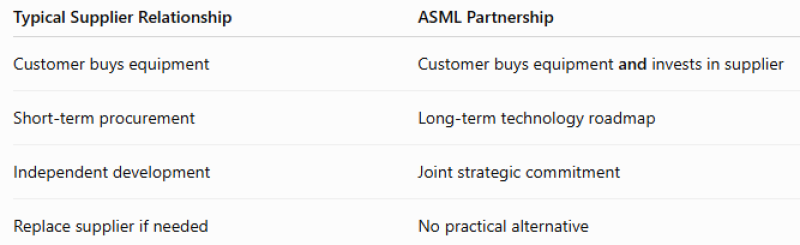
The investments signaled something that markets had begun to understand: ASML was no longer merely another equipment vendor. It had become a strategic dependency.
Fifteen Years Before the First Real Success
Popular accounts of technological breakthroughs often compress decades into a few paragraphs. The history of EUV is a reminder that industrial innovation rarely follows such a neat trajectory.
Prototype systems repeatedly missed performance targets. Light sources lacked sufficient power. Mirrors degraded faster than expected. Throughput remained too low for commercial manufacturing. Every apparent breakthrough exposed another bottleneck elsewhere in the system.
Critics argued that EUV would never leave the laboratory. They were not irrational. Measured against conventional product development timelines, EUV looked like a failure. Measured against the history of fundamental industrial technologies, it looked very different.
By the late 2010s, those years of incremental progress finally converged. Light-source power increased. Reliability improved. Throughput reached commercially viable levels. Semiconductor manufacturers began introducing EUV into high-volume production, initially for selected layers and eventually for the most advanced process nodes.
The technology that had once been dismissed as impractical had become indispensable.
Key Takeaways:
- EUV was not an incremental improvement — it required a completely new technological platform.
- ASML accepted a level of technical and financial risk that larger competitors chose to avoid.
- The company's greatest asset became its ecosystem of specialist partners rather than any single invention.
- Customer investments from Intel, TSMC and Samsung reflected the strategic importance of EUV long before it reached mass production.
- By the time EUV proved commercially viable, ASML had accumulated nearly two decades of experience that no competitor could easily replicate.
Inside the World's Most Complex Machine
There is an old saying among semiconductor engineers that every advanced chip begins with a flash of light. In the era of extreme ultraviolet lithography, that statement is literally true. Every transistor inside an Nvidia GPU, Apple's A-series processor or AMD's latest EPYC server chip starts with an event lasting only a fraction of a second—a microscopic explosion inside a vacuum chamber.
That explosion is carefully orchestrated thousands of times every second. It is not powerful enough to shake the building or produce a visible fireball, yet it represents the heart of the most sophisticated manufacturing process ever developed. Understanding why ASML became irreplaceable requires understanding what actually happens inside one of its machines.
The answer is far more complicated than most people expect.
From Digital Design to Physical Reality
Long before silicon enters an ASML system, chip architects have already spent years designing billions of transistors. These designs exist only as digital layouts—vast collections of geometric patterns describing where every gate, wire and contact should appear on a finished chip.
Turning those digital instructions into physical structures requires repeating the same sequence dozens of times.
A silicon wafer is coated with an ultra-thin layer of photoresist, a light-sensitive chemical similar in principle to photographic film. Selected regions are exposed to light, chemically altered, and then developed. The exposed pattern becomes a template for etching or depositing materials that eventually form transistors.
Modern processors require this process to be repeated layer after layer.
A high-end AI accelerator may contain more than one hundred separate process steps involving lithography. Each layer must align almost perfectly with every previous layer. A positioning error measured in only a few nanometers can reduce manufacturing yield or render entire chips unusable.
Lithography therefore serves two purposes simultaneously. It determines how small transistor features can become, and it determines how accurately every layer aligns with the rest of the device.
Both challenges become exponentially more difficult as transistor dimensions shrink.
One Exposure, Thousands of Engineering Problems
At first glance, exposing a silicon wafer sounds straightforward. Shine light through a mask, project the pattern and move to the next chip. An EUV system performs the same basic task — but only after solving an extraordinary chain of engineering problems.
The process begins with liquid tin.
Inside the source module, molten tin is heated to approximately 250°C before being injected through an ultra-precise nozzle. The system produces around 50,000 droplets every second, each measuring roughly 25 micrometers in diameter. Timing is critical. Every droplet must arrive at exactly the right position within a tolerance measured in micrometers while travelling at high speed through a vacuum.
A high-power carbon dioxide laser then fires two pulses at each droplet.
The first pulse reshapes the droplet from a sphere into a flattened disk. Engineers discovered that this geometry dramatically improves the efficiency of the second pulse, which follows only microseconds later. That second laser strike vaporizes the tin into plasma reaching temperatures approaching 220,000°C — several times hotter than the surface of the Sun.
At this temperature, tin atoms emit radiation across a broad spectrum, including the narrow wavelength that the semiconductor industry desperately needs: 13.5 nanometers.
Generating the light is only the beginning of the journey.
The Journey of a Photon
| Stage | What Happens |
| 1 | Molten tin forms microscopic droplets. |
| 2 | First laser pulse reshapes the droplet. |
| 3 | Second pulse creates plasma at ~220,000°C. |
| 4 | Plasma emits EUV radiation. |
| 5 | Collector mirror captures part of the light. |
| 6 | Beam travels through the optical system. |
| 7 | Pattern is reflected from the photomask. |
| 8 | Projection mirrors reduce the image. |
| 9 | Pattern reaches the wafer. |
What appears as a single manufacturing step actually consists of hundreds of precisely synchronized operations.
Why Ordinary Glass Becomes Useless
Every camera, microscope and telescope depends on lenses. EUV machines cannot use them. Extreme ultraviolet radiation carries enough energy to be absorbed almost instantly by ordinary glass. If engineers attempted to build a conventional optical system, virtually no light would reach the wafer.
The only practical solution is reflection. Even that approach introduces enormous challenges.
A conventional bathroom mirror reflects most visible light with little difficulty. EUV radiation behaves very differently. Instead of polished glass, ASML relies on multilayer mirrors manufactured by Carl Zeiss SMT. Each mirror consists of dozens of alternating layers of molybdenum and silicon, each deposited with atomic-scale precision. These layers create constructive interference that reflects approximately 70% of incoming EUV radiation.
Seventy percent may sound impressive. In reality, it is a serious limitation.
An EUV beam reflects from multiple mirrors before reaching the wafer. Every reflection loses additional energy. After passing through the entire optical path, only a small fraction of the original light remains available for exposure.
Generating enough usable photons therefore became one of the defining engineering challenges of EUV.
Engineering in Perspective
Imagine standing in front of a row of mirrors where each reflection removes 30% of the remaining light. After one reflection, 70% remains. After two, only 49%. After six reflections, less than 12%. Every additional optical surface reduces the available energy.
This explains why increasing the brightness of the light source occupied ASML engineers for nearly two decades. Without sufficient brightness, commercial semiconductor production would simply take too long.
Precision Beyond Human Intuition
Producing light and guiding it through mirrors solves only part of the problem. The wafer itself must move continuously beneath the optical system while remaining aligned with astonishing accuracy. Modern wafer stages travel at speeds approaching one meter per second during scanning exposures. Despite this motion, positioning accuracy is measured in nanometers.
To appreciate that level of precision, consider the following comparison. If a commercial aircraft flying between Amsterdam and New York maintained the same proportional positioning accuracy, it would arrive within a fraction of a millimeter of its intended destination.
Achieving such stability inside a machine weighing more than 150 tonnes requires technologies borrowed from multiple scientific disciplines. Laser interferometers continuously measure position. Magnetic levitation minimizes mechanical friction.
Active vibration isolation compensates for disturbances originating both inside and outside the building. Advanced control software performs millions of calculations every second, constantly correcting tiny deviations before they affect image quality.
The result is a manufacturing platform capable of repeating the same exposure process thousands of times while maintaining nearly identical accuracy across an entire wafer.
The Cleanest Manufacturing Environment on Earth
Contamination is a familiar problem in most industries. Dust scratches paint. Moisture corrodes metal. Oil damages machinery. Inside an EUV system, contamination operates on an entirely different scale. Particles invisible under ordinary lighting can distort transistor patterns.
Molecular films only a few atoms thick gradually reduce mirror reflectivity. Residual gases interfere with plasma generation.
For these reasons, EUV machines operate inside ultra-high vacuum environments where air itself has been almost entirely removed. Engineers wear specialized cleanroom clothing, while sophisticated filtration systems continuously eliminate contaminants introduced during maintenance.
Even under these conditions, contamination never disappears completely.
Instead, it becomes another engineering variable requiring continuous monitoring throughout the system's operational life.
Fact Box
Why Vacuum Matters
EUV light cannot travel through ordinary air. At atmospheric pressure, the beam would be almost completely absorbed before reaching the wafer. Removing air from the optical path is therefore not an optimization — it is a fundamental requirement. Without vacuum technology, EUV lithography would be physically impossible.
Software: The Invisible Machine Inside the Machine
When people think about ASML, they usually imagine lasers, mirrors and precision mechanics.
Yet software has become equally important.
A modern EUV system generates enormous volumes of operational data. Sensors monitor temperature, vibration, pressure, optical alignment, wafer positioning and plasma behaviour simultaneously. Algorithms analyse these measurements in real time, adjusting system parameters before small deviations become manufacturing defects.
The software also integrates with customer production systems, allowing fabrication plants to predict maintenance requirements, optimise throughput and improve yield.
This digital layer transforms lithography equipment from a static industrial machine into an adaptive manufacturing platform. It also explains why copying ASML would require more than duplicating its hardware. The machine embodies decades of accumulated knowledge encoded not only in metal and optics, but also in millions of lines of highly specialised software.
More Than the Sum of Its Parts
It is tempting to identify a single breakthrough that made EUV possible — the mirrors, the plasma source or the laser.
In reality, no individual component explains ASML's dominance. The company's achievement lies in integrating hundreds of frontier technologies into one reliable production system. Each subsystem operates close to the limits of modern engineering. Each depends on the performance of every other subsystem. Failure in one area compromises the entire platform.
That interconnected complexity has become one of ASML's strongest competitive advantages. Developing an equivalent machine no longer means solving one difficult scientific problem. It means mastering dozens of them simultaneously while ensuring they function reliably every hour of every day inside the world's most advanced semiconductor factories.
For that reason, many engineers argue that the true product ASML sells is not lithography equipment. It sells certainty. Certainty that a $25 billion fabrication plant will continue producing chips measured not in millions, but in trillions of transistors, year after year.
What Comes Next
Understanding how the machine works answers only half of the puzzle. The next question is even more interesting:
If the technology is so valuable, why hasn't another company copied it?
The answer has surprisingly little to do with patents — and almost everything to do with an industrial ecosystem that took decades to build. Part V explores that ecosystem, from Zeiss and TRUMPF to hundreds of invisible suppliers whose technologies collectively form one of the deepest competitive moats in modern manufacturing.
 Artem Voloskovets